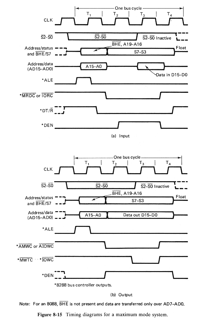
The timing diagram for input and output on a maximum mode
system are given in Fig.8-15. The /S0, /S1 and /S2 bits
are set just prior to the beginning of the bus cycle.
Interrupt acknowledgment signals are the same as in the
minimum mode case except that a 0 is applied to the /LOCK
pin from T2 of the first bus cycle to T2 of the second
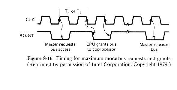
bus cycle. Bus requests and grants are handled
differently, however, and the timing on an /RQ / /GT pin is shown in
Fig.8-16.
| PRETHODNA FOLIJA | SADRZAJ | SLEDECA FOLIJA |