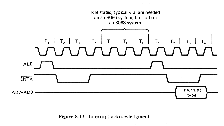
The timing diagram for an interrupt acknowledge is shown
in Fig.8-13. If an interrupt request has been recognized
during the previous bus cycle and an instruction has just
been completed, then a negative pulse will be applied to
/INTA during the current bus cycle and the next bus cycle.
Each of these pulses will extend from T2 to T4. Upon
receiving the second pulse, the interface accepting the
acknowledgment will put the interrupt type on AD7-AD0,
which are floated the rest of the time during the two
bus cycles. The type will be available from T2 to T4.
Figure 8-14 shows the timing of a bus request and bus
grant in a minimum mode system. The HOLD pin is tested
at the leading edge of each clock pulse. If a HOLD signal
is received by the processor before T4 or during a T1
state, then the CPU activates HLDA and the succeeding bus
cycle will be given to the requesting master until that
master drops its request. The lowered request is
detested at the rising edge of the next clock cycle and
the HLDA signal is dropped at the trailing edge of that
clock cycle. While HLDA is 1, all of the processor's
three-state outputs are put in their high-impedance state.
Instructions already in
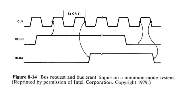
the instruction queue will continue to be executed until
one of them requires the use of the bus. The instruction
MOV AX, BXcould execute completely, but
MOV AX, NUMBERwould only execute until it is necessary to bring in data from the location NUMBER.
| PRETHODNA FOLIJA | SADRZAJ | SLEDECA FOLIJA |