It is assumed that the chip enable and output enable pins are CE and \CS, respectively.The block-diagram in Fig.10-11 shows the logic needed to generate the chip enable and the refresh address signals during a memory refresh.
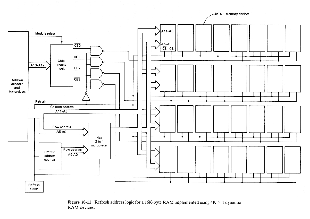
Consider a memory module of 16K bytes implemented by 4K x 1 dynamic RAMs.
The memory device array consists of four rows and eight columns.Each chip
has 64 rows and 64 columns of memory cells and has separate row address
(6 bits) and column address (6 bits) pins.
It is assumed that the chip enable and output enable pins are CE and \CS,
respectively.The block-diagram in Fig.10-11 shows the logic needed to
generate the chip enable and the refresh address signals during a memory
refresh.
| PRETHODNA FOLIJA | SADRZAJ | SLEDECA FOLIJA |