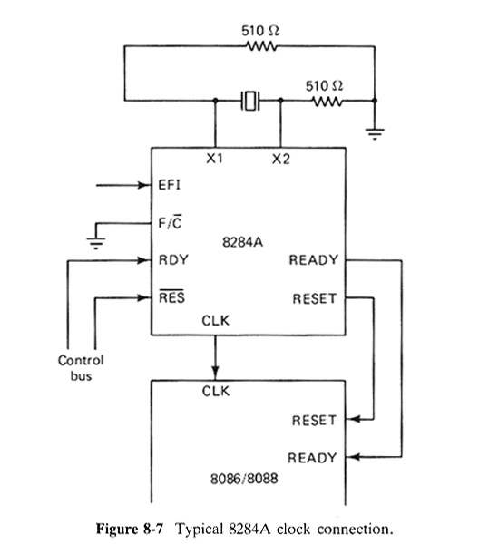
The third component, other than the processor, that appears in Fig.8-4 is an 8284A clock generator. This device, which is actually more than just a clock, is detailed in Fig.8-7.
type of transfer according to the following table:
M / /IO    /RD     /WR
  0         0       1   I/O read
  0         1       0   I/O write
  1         0       1   Memory read
  1         1       0   Memory write
/INTA signal consists of two negative pulses output during two consecutive bus cycles. The first puls informs the interface that its request has been recognized, and upon receipt of the second pulse, the interface is to send the interrupt type to the processor over the data bus.
| PRETHODNA FOLIJA | SADRZAJ | SLEDECA FOLIJA |