Except for pins 28 and 34 the two processors have
the same control pin definitions. Pin 28 differs in the
minimum mode. For the 8088 this minimum mode signal is
inverted from that of the 8086, so that the 8088 is
compatible with the Intel 8085 microcomputer chip.
On the 8086, pin 34(/BHE) designates whether or not at
least 1 byte of a transfer is to be made on AD15 through
AD8. A 0 on this pin indicates that the more significant
data lines are to be used; otherwise, only AD7 through
AD0 are used.
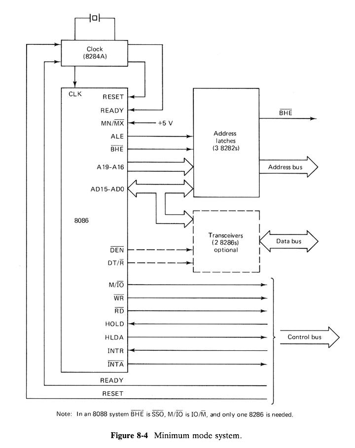
A processor is in minimum mode when its MN / /MX pin is
strapped to +5V. The definitions for pins 24 through 31
for the minimum moda are given in Fig.8-3 and
a typical minimum mode configuration is shown in Fig.8-4.
| Figure 8-3 Pin definitions for the minimum mode | |||
| Pin(s) | Symbol | In/Out(3 State) | Description |
| 24 | /INTA | O-3 | Indicates recognition of an interrupt request. Consists of two negative going pulses in two consecutive bus cycles. |
| 25 | ALE | O | Outputs a pulse at the beginning of the bus cycle and is to indicate an address is available on the address pins. |
| 26 | /DEN | O-3 | Output during the latter portion of the bus cycle and is to inform the transceivers that the CPU is ready to send or receive data. |
| 27 | DT / /R | O-3 | Indicates to the set of transceivers whether they art to transmit (1) or receive (0) data. |
| 28 | M / /IO | O-3 | Distinguishes a memory transfer from an I/O transfer. For a memory transfer it is 1. (For the 8088, the symbol is IO / /M and a 1 indicates an I/O transfer. |
| 29 | /WR | O-3 | When 0, it indicates a write operation is being performed. It is used in conjuction with pins 28 (M / /IO) and 32 (/RD) to specify the type of transfer |
| 30 | HLDA | O | Outputs a bus grant to a requesting master. Pins with trisate gates are put in high impedance state while HLDA=1. |
| 31 | HOLD | I | Receivec bus requests from bus masters. The 8086/8088 will not gain control of the bus until this signal is dropped. |
| PRETHODNA FOLIJA | SADRZAJ | SLEDECA FOLIJA |