When this is done, the bit being output not only depends on the signals on the address lines, but also depends on which chips receive the chip enable signal.Each row in the array is connected to a row enable line and the row enable lines are activated by higher-order address bits, which for this example are bits A11 and A10.
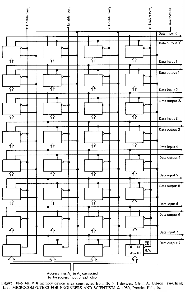
In summary, if the address contains 16 bits, A15-A12 would select the module, A11 and A10 would select the row, and A9-A0 would select the bits in the devices which constitute the addressed byte.