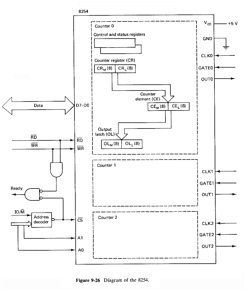
The registers can be accessed according to the following table:
The registers can be accessed according to the following table:
      __   __   __
      CS   RD   WR   A1   A0          Transfer

      0    1    0    0    0        To counter 0 CR
      0    1    0    0    1        To counter 1 CR
      0    1    0    1    0        To counter 2 CR
      0    1    0    1    1        To a control register or indicates a command
      0    0    1    0    0        From counter 0 OL or status register
      0    0    1    0    1        From counter 1 OL or status register
      0    0    1    1    0        From counter 2 OL or status register
All other combinations result in the data pins being put into their
high-impedance state.When A1=A0=1, whether a control register is being written
or a command is being given depends on the MSBs of the byte being output.
| PRETHODNA FOLIJA | SADRZAJ | SLEDECA FOLIJA |