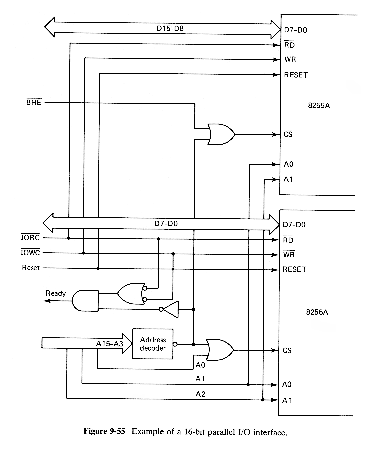
The A2 and A1 lines in the address bus are connected to the A1 and A0 pins of both 825As: thus the 16-bit ports are formed from the pairs of ports A,B,C and the control/status registers.
The lower 8255A occupies 4 consecutive even addresses and the upper 8255A occupies 4 consecutive odd addresses.If bits A15-A3 match the address designed into the address decoder, then the decoder will emit a 0 chip select signal.
For the lower 8255A, if both the chip select and A0 signals are 0, then a 0 is applied to \CS.For the upper 8255A, both the chip select and \BHE signals must be 0 in order for a 0 to be sent to the \CS.(Therefore, it is possible to address the 8255As individually.).The read,write and reset control lines are connected to the \RD,\WR and RESET pins of both of the 8255As and a ready signal is returned if either \CS signal is active.
One other alternative in interface design is to treat registers of an I/O device as memory locations.