7.6 A Read/Write RAM Interface Example
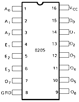
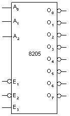
Some special decoder IC's have been produced which help simplify the design of address decoding circuitry. One such decoder in common use is the 8205 (alias 74LS138). Pertinent data for this IC is listed below.
PIN CONFIGURATION
 | LOGIC SYMBOL
 |
PIN NAMES
| A0-A2 | Address Inputs |
| E1-E3 | Enable Inputs |
| O0-O7 | Decoded Outputs |
| ADDRESS | ENABLE | OUTPUTS |
|---|
|
|
|
|
| L | L | L |
| H | L | L |
| L | H | L |
| H | H | L |
| L | L | H |
| H | L | H |
| L | H | H |
| H | H | H |
| X | X | X |
| X | X | X |
| X | X | X |
| X | X | X |
| X | X | X |
| X | X | X |
| X | X | X |
|
| L | L | H |
| L | L | H |
| L | L | H |
| L | L | H |
| L | L | H |
| L | L | H |
| L | L | H |
| L | L | H |
| L | L | L |
| H | L | L |
| L | H | L |
| H | H | L |
| H | L | H |
| L | H | H |
| H | H | H |
|
| L | H | H | H | H | H | H | H |
| H | L | H | H | H | H | H | H |
| H | H | L | H | H | H | H | H |
| H | H | H | L | H | H | H | H |
| H | H | H | H | L | H | H | H |
| H | H | H | H | H | L | H | H |
| H | H | H | H | H | H | L | H |
| H | H | H | H | H | H | H | L |
| H | H | H | H | H | H | H | H |
| H | H | H | H | H | H | H | H |
| H | H | H | H | H | H | H | H |
| H | H | H | H | H | H | H | H |
| H | H | H | H | H | H | H | H |
| H | H | H | H | H | H | H | H |
| H | H | H | H | H | H | H | H |
|
|
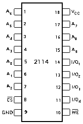
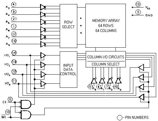
A commonly-used static RAM IC, the 2114, is illustrated below. Containing 4K bits of storage, it is organized as 1024 four-bit memory locations. Note the different speed/power varieties of this memory IC which are available.
| 2114-2 | 2114-3 | 2114 | 2114L3 | 2114L |
|---|
| Max. Access Time (ns) | 200 | 300 | 450 | 300 | 450 |
|---|
| Max. Power Dissipation (mw) | 710 | 710 | 710 | 370 | 370 |
|---|
PIN CONFIGURATION
 | LOGIC SYMBOL
 |
PIN NAMES
| A0-A9 | Address Inputs | | VCC | Power (+5V) |
| WE | Write Enable | | GND | Ground |
| CS | Chip Select |
| I/O1-I/O4 | Data Input/Output |
|
BLOCK DIAGRAM
 |
Table of Contents | Next page | Previous page
This is page 6.
